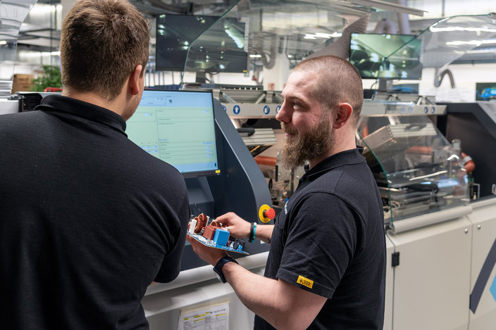
Technology Days planned and held exclusively for companies
For technology focused companies we offer customer-specific Technology Days, which are arranged according to individual topics and needs. Since the seminars are organized and conducted exclusively for your company, the theoretical and practical sessions can be tailored exactly to the needs of your employees. In addition, the exchange of knowledge and experience among your own employees across departments and locations is stimulated. The focus of the two-day intensive course is to observe and analyze all boundary conditions affecting the soldering process.
Technology days for auditors
Exclusively for users who are not directly involved in the soldering processes, we offer Technology Days that deal specifically with the process knowledge that is relevant to you. Our experts will give you an insight into our technology, processes and explain, for example, what needs to be taken into account when auditing suppliers in these processes. In addition, we take the time to explicitly address your questions about joining technology.
Design your technology days from the following modules
SOLDER PASTE PRINTING
REFLOW SOLDERING
REWORK
WAVE & SELECTIVE SOLDERING
PRESS-FIT
HAND SOLDERING
SOLDERING TECHNOLOGY FOR HIGH RELIABILITY ELECTRONICS
SOLDERING TECHNOLOGY FOR HIGH RELIABILITY ELECTRONICS
- Design challenges for high reliability assemblies and devices
- Optimized PCB layout under thermo-dynamic aspects
- Flexible system concepts which, considering throughput and variant range, allow precise adaptation of the process parameters to the individual solder joints
DESIGN
OPTICAL INSPECTION
Fee
- Basic: 999,- € per person plus VAT
- Exam fee: 100,- € per person plus VAT
Optional examination for all participants with subsequent issue of certificate. Seminar participants who do not take the exam will receive a certificate of attendance.
References: Automotive manufacturers, industrial electronics, drive technology, consumer electronics

